Product Introduction
Silicon carbide (SiC) targets are manufactured from high-purity powders, offering excellent resistance to high temperatures and corrosion, alongside superior chemical stability and thermal conductivity. These properties make them especially suitable for depositing high-performance thin films under harsh operating conditions. They are vital functional materials widely used across the semiconductor, photovoltaic, and optical industries.
Key Advantages of Silicon Carbide Targets
High Purity, Cleaner Films
Silicon carbide targets use high-purity SiC raw materials with metal impurity content below 100 ppm. The deposited films have fewer defects and contaminations, with stable electrical and optical properties, making them suitable for high-end electronic devices.
Ultra-high hardness and wear resistance
The target is resistant to peeling and cracking under high-power sputtering conditions, extending target lifetime by more than 30% as compared with conventional ceramic targets. This reduces particle contamination and improves production yield.
Excellent Thermal Conductivity and Thermal Shock Resistance
It enables rapid heat dissipation and allows higher power-density sputtering. The target is resistant to cracking caused by thermal shock, making it suitable for long-term continuous deposition.
Dense and uniform structure, consistent film quality
Silicon carbide targets feature a high density and uniform particle distribution, enabling high deposition rates and excellent film thickness uniformity. Stable quality can be maintained even for large-size targets.
Main Application Areas of Silicon Carbide Targets
Semiconductor Manufacturing
Used for thin film deposition in power devices, RF devices, and MEMS sensors. Dense and highly insulating films are formed via magnetron sputtering and related processes, improving device breakdown voltage, temperature resistance, and stability.
Display Panels
Silicon carbide (SiC) targets are utilized as robust hard protective layers or buffer layers in modern displays, including LCD, OLED, Micro-LED, and flexible technologies. These layers enhance scratch resistance and chemical stability while ensuring crucial optical transmittance and maintaining touch sensitivity
Photovoltaic Industry
SiC is utilized as anti-reflection layers, protective films, or buffer layers in both crystalline silicon and thin-film solar cells. These applications improve light absorption efficiency, significantly reduce reflection losses, and enhance the long-term stability and overall durability of the devices.
Optical Device Manufacturing
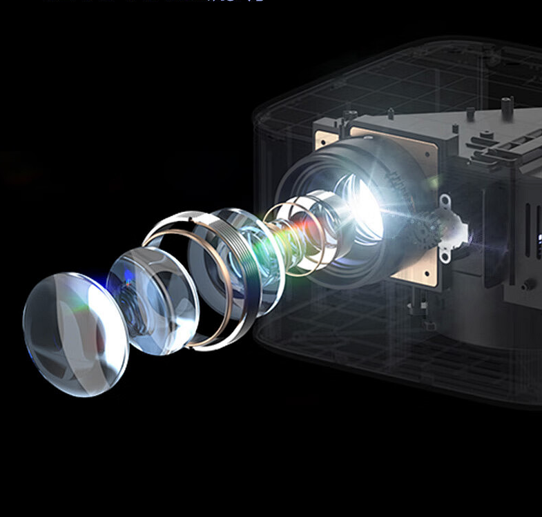
SiC is used for coating lenses, filters, prisms, and other optical components. Film refractive index and transmittance can be controlled to achieve anti-reflection, filtering, or high-reflection functions, suitable for laser optics and aerospace applications.
Decorative Coatings
Forms high-hardness, wear-resistant coatings on the surfaces of mobile phones, watches, automotive interiors, and precision components. This application provides an attractive metallic appearance while extending product service life.
Technical Characteristics

Purity
99.9%-99.999%
Density
3.21 g/cm³
Application Fields

Semiconductor Manufacturing

Display Panels
Optical Device Manufacturing

Decorative Coatings
Contact Us