Product Introduction
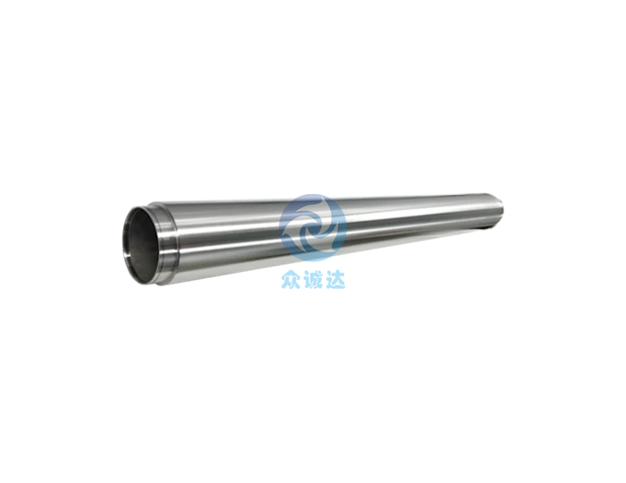
Copper-nickel targets are alloy targets made from high-purity copper and nickel, processed through precision melting, rolling, machining, and other steps under vacuum or protective atmospheres. By carefully controlling the alloy composition, impurity content, and microstructure, it retains copper's excellent electrical and thermal conductivity while incorporating nickel's high strength and corrosion resistance, making it a commonly used functional target material in various industries.
Key Advantages of Copper-Nickel Targets
Excellent Electrical and Thermal Conductivity
High-purity copper imparts low resistivity and high thermal conductivity to the target, ensuring that the deposited films maintain stable electrical conductivity and heat dissipation under high-frequency and high-power conditions, making it ideal for power devices and large-area substrates.
Strong corrosion and wear resistance
Nickel enhances the target and film’s oxidation and corrosion resistance, specifically under high humidity. It forms a dense passivation layer that significantly extends the operational lifespan of both the film and the device.
Dense Film Layers and High Adhesion
The sputtered films have smooth surfaces, fine particles, uniform thickness, and excellent adhesion, which help improve yield and stability of the finished products.
Excellent mechanical properties
Typically, copper-nickel targets have high hardness and strength, maintaining stability and durability during sputtering, reducing deformation and damage caused by sputtering, ensuring smooth sputtering processes.
Main Applications of Copper-Nickel Targets
Semiconductor Manufacturing
Copper-nickel alloy targets are commonly used for depositing key metal layers such as interconnects and contact electrodes during chip manufacturing. Through magnetron sputtering or PVD processes, a dense and highly conductive thin film is formed on the wafer surface, ensuring efficient and stable electrical connections between circuits to meet the reliability and performance demands of advanced processes.Display Industry
Copper-nickel targets are essential for fabricating electrode and thin-film transistor (TFT) layers in LCD and OLED displays. Their uniform deposition facilitates high-adhesion, low-resistance films that significantly enhance response speed, brightness uniformity, and overall picture quality of display panels.
Photovoltaic Industry
copper-nickel targets are utilized to deposit high-performance electrodes and barrier layers for crystalline silicon and thin-film solar cells. These sputtered films provide a unique combination of high electrical conductivity and superior corrosion resistance, directly enhancing power conversion efficiency (PCE). By stabilizing the interfacial electrical contacts, these layers ensure long-term operational stability and significantly extend the service life of photovoltaic modules.
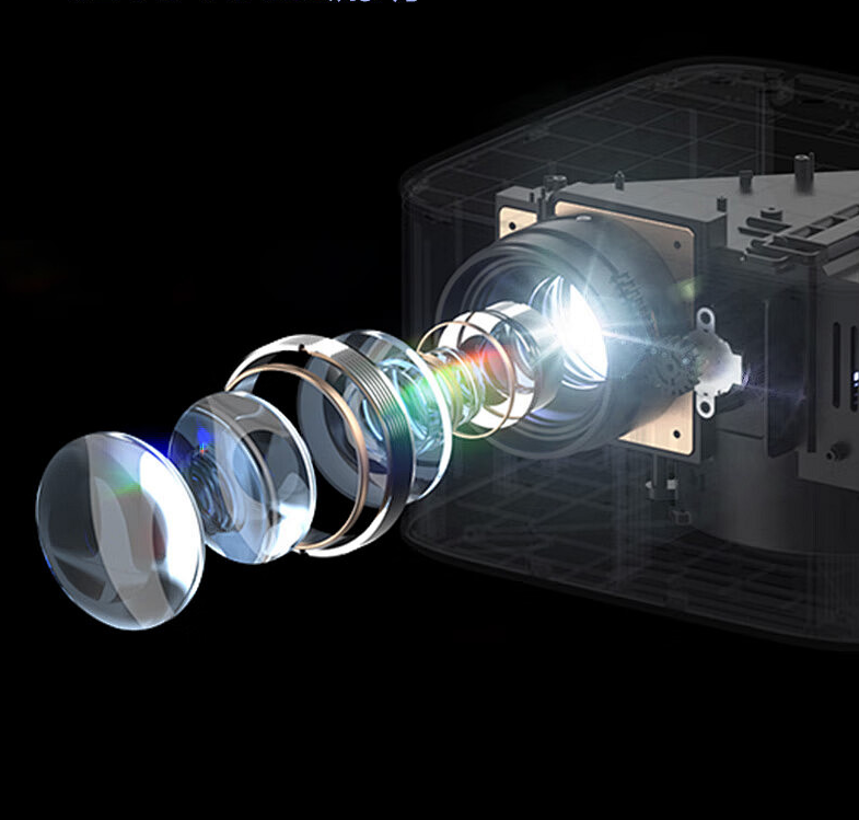
Optical Device Manufacturing
Copper-nickel targets are utilized to deposit high-precision coatings on lenses and filters, offering exceptional spectral control. Modulating film thickness and deposition parameters, manufacturers can precisely tune reflectance, transmittance, and absorption levels. This level of technical accuracy is essential for high-end optical systems, including telescopes, microscopes, and advanced telecommunications infrastructure.
Technical characteristics

Purity
99.9%-99.99%
Proportioning
Customizable ratio
Application Fields

Semiconductor Manufacturing

Display Industry

Photovoltaic Industry
Optical Device Manufacturing
Contact Us