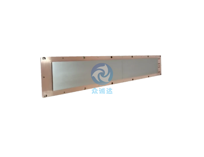
Product Introduction
Engineered from high-purity powders this alloy combines the exceptional hardness, thermal resilience, and high melting point characteristic of molybdenum with the superior electrical conductivity and chemical inertness of niobium. MoNb targets are used to prepare wear-resistant, high-temperature-resistant, and corrosion-resistant functional films, with applications in semiconductor, optical, energy, and high-end decorative coating fields. The MoNb films produced by sputtering have high density, good adhesion, and stable physical and chemical properties.
Core Advantages of MoNb Target
High Temperature Resistance
The molybdenum content provides a high melting point and good thermal stability, allowing the film to remain stable during high-temperature sputtering processes, suitable for high-power deposition.
Strong Corrosion Resistance
Niobium enhances film resistance against acid, alkali, and oxidation environments, extending the lifespan of the films and devices.
Good Electrical Conductivity
The alloy film has stable electrical conductivity, making it suitable for use in electronic devices, functional films, and transparent conductive films.
High Hardness and Wear Resistance
MoNb films have high hardness and wear resistance, suitable for protective coatings and high-end decorative coatings, enhancing durability.
Good Film Density
Sputtered films are uniform having strong adhesion which ensure film stability in diverse applications.
Main Applications of MoNb Target
Semiconductor Manufacturing
MoNb targets can be used to prepare conductive layers, interconnect layers, or shielding layers, providing stable electrical performance and long-term reliability for semiconductor devices and electronic components.Display Panels
Used to deposit functional films such as transparent electrode auxiliary layers, gate electrodes, or interconnect lines in LCD, OLED, and Mini/Micro LED display panels. Core advantages: good flexibility, strong interface adhesion with transparent conductive layers (ITO/IZO), and high sputtering uniformity.
Photovoltaic Industry
Mainly used for back electrodes or conductive backplates in thin-film photovoltaic cells (such as CIGS, CdTe cells). Core advantages: high temperature resistance, resistance to photovoltaic electrolyte corrosion, and low contact resistance.
Aerospace
MoNb films have high hardness, high-temperature resistance, and corrosion resistance, making them suitable for surface protection of aerospace and high-temperature industrial equipment, extending the lifespan of critical components.
Technical characteristics

Purity
99.9%-99.99%
Proportioning
Customizable Ratio
Application Fields

Semiconductor Manufacturing

Display Panels

Photovoltaic Industry

Aerospace
Contact Us