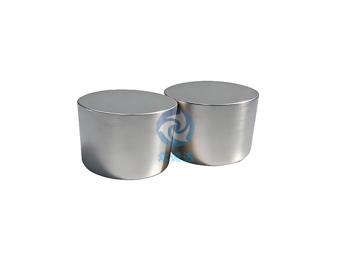
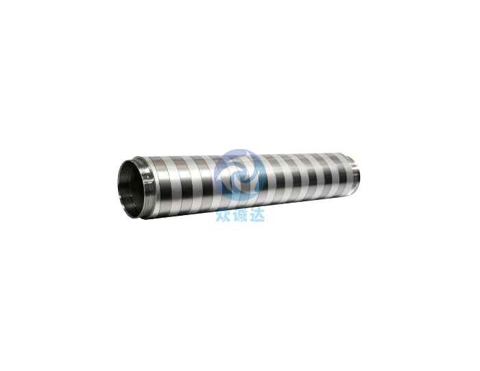
Product Introduction
Fabricated from high-purity rare earth metal, our ytterbium (Yb) targets leverage the element's inherent ductility and low vapor pressure to ensure exceptional process stability. Even under rigorous high-vacuum and high-temperature conditions, these targets maintain their integrity, facilitating the deposition of dense, uniform, and highly adherent functional thin films for advanced technological applications.
Ytterbium Target’s Exceptional Properties
High Purity, Low Impurities
Manufactured from ultra-high purity ytterbium, the targets feature a low impurity profile that significantly minimizes particulate contamination and pinhole formation. This results in superior film density, exceptional uniformity, and enhanced structural stability across the entire substrate..
High Density and Uniformity
Yb targets feature a refined microstructure and high density, which ensures superior stability during the sputtering process and guarantees highly uniform film thickness across the substrate.
Good Ductility and Workability
Ytterbium metal is soft and highly ductile, making it easy to process into various specifications and shapes (e.g., round, rectangular, and ring targets) to meet the needs of different equipment.
Excellent Chemical Stability
It is stable in high vacuum and high-temperature sputtering conditions, which makes it resistant to reactions with working gases or substrates, ensuring stable and pure films.
Unique Optoelectronic and Magnetic Properties
Ytterbium elements can impart unique optical, electrical, or magnetic properties to the films, providing differentiated functionality and enhancing product value.
Wide Applications of Ytterbium Sputtering Specimens
Integrated Circuits and Semiconductor Industry
Contact Layers and Barrier Layers: As transistor sizes shrink to the nanometer scale in advanced semiconductor chips (such as logic chips and memory), a traditional silicide contacts can no longer meet low-resistance requirements. Ytterbium metal, with its low work function, can be used as the ohmic contact layer for N-type transistors, effectively reducing the contact resistance between the source, drain, and channel, thereby improving device performance and operating speed.
Organic Light Emitting Diodes (OLEDs)
The work function of ytterbium (Yb) provides an ideal alignment with the LUMO energy levels of OLED organic materials. Consequently, ytterbium thin films are frequently utilized as electron injection layers or cathode components. By facilitating efficient electron injection into the emissive layer, they maximize electroluminescent conversion efficiency while significantly reducing operating voltage. Furthermore, ytterbium’s superior atmospheric stability compared to highly reactive metals like calcium enhances the overall device longevity.
Solar Cells
In new photovoltaic devices like perovskite solar cells, ytterbium thin films can serve as an effective electron transport layer or electrode interface modification layer, which helps in extracting electrons, enhancing open-circuit voltage, and filling factors, ultimately improving photoelectric conversion efficiency.
Decorative and Functional Coatings
Metallic ytterbium has a silvery-white color with a slight yellowish hue. By sputtering ytterbium targets, films with special metallic luster and color can be deposited on the surfaces of consumer goods such as eyeglass frames, watches, and mobile phone housings, offering both aesthetic appeal and wear-resistance, corrosion resistance.
Technical Characteristics

Purity
99.9%-99.99%
Relative Density
≥99%
Application Fields

Integrated Circuits and Semiconductor Industry
Organic Light Emitting Diodes (OLEDs)

Solar Cells

Decorative and Functional Coatings
Contact Us