Product Introduction
High Purity Copper Target, Custom/Planner/Rotary Copper Targets, Copper Target Supplier for Sputtering Coating
The physical properties of materials directly determine the film quality and production efficiency in vacuum sputtering coating. Copper targets, with their inherent excellent conductivity and outstanding thermal conductivity, have become a "key material" in high-end manufacturing fields such as semiconductor manufacturing, display panels, photovoltaic industry, and power batteries. Their unique performance advantages not only ensure the stability and efficiency of the sputtering process but also endow the coated products with excellent functionality and reliability.
Core Advantages of Copper Target:Purity and Grain Size
Ultra-high Purity,Extremely Low Impurities
Using high-purity electrolysis copper ranging from 99.9% (3N) to 99.9999% (6N) as raw material, multi-step purification processes (electrolytic refining, zone refining) are used to strictly control the impurities such as oxygen, sulfur, iron, etc., ensuring uniform and defect-free sputtered films that meet the performance requirements of precision electronic components.Grain Size Uniformity
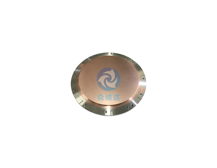
Copper targets exhibit tightly arranged grains with a consistent orientation (texture) under microscopic inspection. This optimized microstructure ensures high stability during the sputtering process and guarantees uniform film quality.
Excellent Physical Properties, Stable Sputtering
Copper is a reddish-orange metal with a melting point of 1083°C, density of 8.96g/cm3, and boiling point of 2567 °C. Characterized by superior thermal and electrical conductivity, copper targets facilitate rapid heat dissipation during high-frequency sputtering. This effectively prevents deformation or cracking caused by localized thermal stress, ensuring a continuous, stable, and high-yield deposition process..Precision Forming, Strong Compatibility
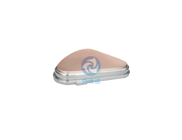
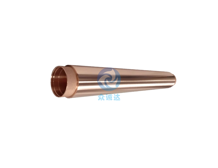
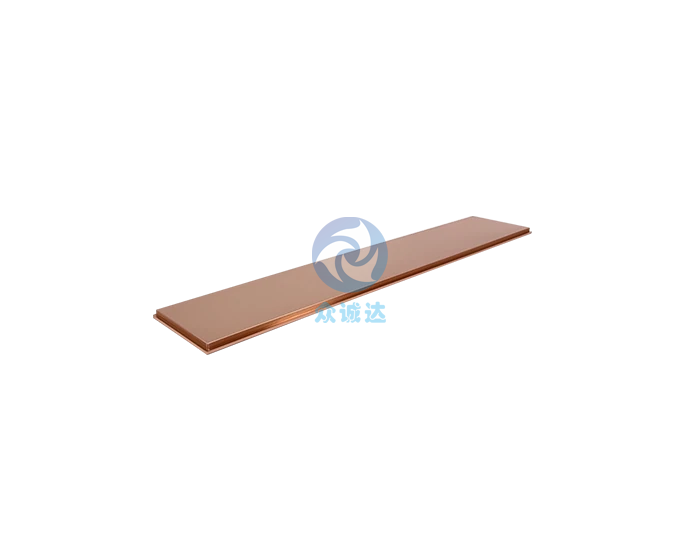
Supports customization of various specifications such as flat targets, rotary targets, and customized shapes, with size accuracy controlled within ±0.1mm. The target surface roughness is Ra ≤ 0.8μm, perfectly compatible with mainstream sputtering equipment such as magnetron sputtering and ion beam sputtering, reducing arcing phenomena during sputtering.
Main Application Fields of Copper Target
Semiconductor Manufacturing
Copper targets are widely used in the metal interconnect layers (such as Cu interconnects) in semiconductor chip manufacturing. With superior electrical and thermal conductivity they effectively reduce resistance and power consumption, making them an indispensable key material in advanced processes.
Display Panels
Copper targets are often used to form conductive wiring layers in the production of LCD, OLED, and other flat-panel displays. Copper has a lower resistance which improves display response speed and energy efficiency as compared to traditional materials.Photovoltaic Industry
Copper targets play a critical role in the fabrication of CIGS (Copper Indium Gallium Selenide) thin-film solar cells. Utilized in the formation of back electrodes and intermediate conductive layers, they contribute significantly to superior photoelectric conversion efficiency and long-term device stability.Power Batteries
Copper targets are also used in the sputtering coating treatment of lithium battery electrodes, enhancing electrode adhesion and conductivity, helping to improve battery cycle life and energy density.
Technical Characteristics

Purity
99.9% (3N) to 99.9999% (6N)
Grains
The grain size of copper targets is controlled in the range of 20-100μm, ensuring uniform grain distribution and consistent orientation. This not only helps optimize sputtering performance but also ensures excellent electrical conductivity and thermal conductivity.
Low Oxygen Content
Oxygen content is less than 10 ppm.
Application Fields

Semiconductor Manufacturing

Display Panels

Photovoltaic Industry
动力电池Power Batteries
Contact Us